Applied Materials Unveils Next-Gen Chipmaking Products to Supercharge AI Performance
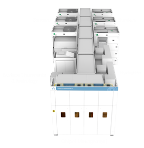
- Kinex™ is the industry’s first integrated die-to-wafer hybrid bonding system; enables production of higher performance, lower power advanced logic and memory chips
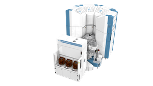
- Xtera™ system enables higher performance Gate-All-Around transistors at 2nm and beyond by depositing void-free, uniform epitaxial layers
-
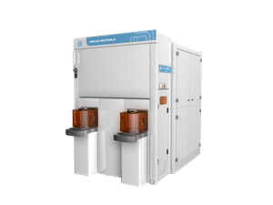
PROVision™ 10 eBeam metrology system improves yield of complex 3D chips by providing sub-nanometer resolution, fast throughput and deep imaging
SANTA CLARA, Calif., Oct. 07, 2025 (GLOBE NEWSWIRE) -- Applied Materials, Inc. today introduced new semiconductor manufacturing systems that boost the performance of advanced logic and memory chips foundational to AI computing. The new products target three critical areas in the race to deliver ever more powerful AI chips: leading-edge logic including Gate-All-Around (GAA) transistors, high-performance DRAM including high-bandwidth memory (HBM), and advanced packaging to create highly integrated systems-in-a-package that optimize chip performance, power consumption and cost.
“As chips become more complex, Applied is focused on driving materials engineering breakthroughs to provide the performance and power-efficiency improvements needed to scale AI,” said Dr. Prabu Raja, President of the Semiconductor Products Group at Applied Materials. “We are collaborating earlier and deeper with our customers to co-develop solutions that accelerate chipmaker roadmaps and enable major device inflections in logic, memory and advanced packaging.”
New Kinex™ Bonding System Enables Production of Higher Performance, Lower Power Advanced Logic and Memory Chips
To optimize performance and power efficiency, today’s leading GPUs and high-performance computing (HPC) chips use advanced packaging schemes to combine multiple chiplets into complex systems. Hybrid bonding is an emerging chip-stacking technology that uses direct copper-to-copper bonds, resulting in significant improvements in overall performance, power consumption and cost.
Increasingly complex chip packages create challenges for hybrid bonding in high-volume manufacturing. To accelerate the use of hybrid bonding in advanced logic and memory chips, Applied Materials, in collaboration with BE Semiconductor Industries N.V. (Besi), developed the Kinex™ Bonding system – the industry’s first integrated die-to-wafer hybrid bonder. The system brings together Applied’s expertise in front-end wafer and chip processing with high levels of bonding accuracy and speed from Besi’s leading die placement, interconnect and assembly solutions.
The Kinex system integrates all the critical hybrid bonding process steps into one system, offering several major advantages compared to non-integrated approaches:
- Better management of complex multi-die packages because of superior die-level tracing
- Smaller interconnect pitches enabled by high-accuracy bonding and clean, controlled environment
- Improved bonding consistency and quality through precise control over the queue time between hybrid bonding process steps
- Faster overlay measurement and drift detection achieved by integrated, in-line metrology
The Kinex system is being used by multiple leading-edge logic, memory and OSAT* customers. An animation of the system can be viewed here.
New Centura™ Xtera™ Epi System Enables Higher Performance GAA Transistors at 2nm and Beyond
Among the most critical features affecting the performance and reliability of today’s state-of-the-art GAA transistors are the source and drain structures, which form the transistor channel. The source and drain are created by precisely depositing materials in deep trenches using an epitaxial (epi) process. Filling the high aspect ratio source/drain trenches of 3D GAA transistors using conventional epi is challenging and can lead to voids and uneven growth which reduces performance and reliability.
To solve this challenge and enable maximum chip performance, Applied Materials developed the Centura™ Xtera™ Epi system. The Xtera system features a unique low-volume chamber architecture which includes integrated pre-clean and etch processes to enable void-free GAA source-drain structures with 50 percent lower gas usage than conventional epi. The system’s innovative deposition-etch process continuously adjusts the trench opening as material grows on the side walls and bottom of the trench, optimizing epi growth across the billions of transistors on a wafer, void free with a greater than 40-percent improvement in cell-to-cell uniformity.
The Xtera system is being adopted by leading logic and memory chipmakers. An animation of the system’s capabilities can be viewed here.
Introducing PROVision™ 10 eBeam Metrology System That Improves Yield of Complex 3D Chips
“The increased use of 3D architectures in logic and memory is creating new metrology challenges that are pushing optical technology to the limits,” said Keith Wells, Group Vice President of Imaging and Process Control at Applied Materials. “Applied is extending its eBeam leadership with breakthroughs in imaging resolution, deep into the 3D architecture at high throughput, giving chipmakers the ability to obtain precise measurements and accelerate yield of complex chip designs.”
The new PROVision™ 10 is a cutting-edge eBeam metrology system purpose-built for advanced logic chips – including GAA transistor and Backside Power Delivery architectures – as well as next-generation DRAM and 3D NAND chips. It is the industry’s first metrology system to feature cold field emission (CFE) technology, which increases nanoscale image resolution by up to 50 percent and imaging speed by up to 10X compared to conventional thermal field emission (TFE) technology. The PROVision 10 system’s sub-nanometer imaging capabilities allow it to see through multiple layers of 3D chips and provide an integrative, multi-layer image. The system enables direct on-device overlay measurements and precise critical dimension (CD) metrology, beyond the limits of traditional optical systems. Its unique capabilities support key process control tasks, such as EUV layer overlay and nanosheet measurement and epi void detection in GAA transistors, making it a critical tool for 2nm and beyond, as well as HBM integration.
The PROVision 10 system is being used by multiple leading logic and memory chipmakers.
A media kit with additional information on the Kinex, Xtera and PROVision 10 systems is available on the Applied Materials website.
The new systems, along with other innovations for making future AI chips, will be discussed at Applied’s SEMICON West 2025 Technology Breakfast. The presentation from the event will be available on the Applied Materials website at: https://ir.appliedmaterials.com on Tuesday, Oct. 7, 2025 at 9:00 a.m. ET / 6:00 a.m. PT.
*OSAT = Outsourced Semiconductor Assembly and Test
About Applied Materials
Applied Materials, Inc. (Nasdaq: AMAT) is the leader in materials engineering solutions that are at the foundation of virtually every new semiconductor and advanced display in the world. The technology we create is essential to advancing AI and accelerating the commercialization of next-generation chips. At Applied, we push the boundaries of science and engineering to deliver material innovation that changes the world. Learn more at www.appliedmaterials.com.
Contact:
Ricky Gradwohl (Media) 408.235.4676
Investor Relations (Financial Community) 408.986.7977
Photos accompanying this announcement are available at:
https://www.globenewswire.com/NewsRoom/AttachmentNg/626c6ce9-6656-4f78-a631-2027e6f494e0
https://www.globenewswire.com/NewsRoom/AttachmentNg/6df27bd3-91a6-4dfa-b688-775b21600b6b
https://www.globenewswire.com/NewsRoom/AttachmentNg/f8c6637e-bd9e-4107-8641-4d8eb479e63d

Kinex™ Bonding System
The Kinex™ Bonding system is the industry’s first integrated die-to-wafer hybrid bonder. It enables production of higher performance, lower power advanced logic and memory chips by integrating all the critical hybrid bonding process steps into one system.
Centura™ Xtera™ Epi System
The Xtera™ Epi system enables higher performance Gate-All-Around transistors at 2nm and beyond by depositing void-free, uniform epitaxial layers.
PROVision™ 10 eBeam Metrology System
The PROVision™ 10 eBeam metrology system improves yield of complex 3D chips by providing sub-nanometer resolution, fast throughput and deep imaging.
Legal Disclaimer:
EIN Presswire provides this news content "as is" without warranty of any kind. We do not accept any responsibility or liability for the accuracy, content, images, videos, licenses, completeness, legality, or reliability of the information contained in this article. If you have any complaints or copyright issues related to this article, kindly contact the author above.


